Imagine a world where cutting semiconductor wafers is precise and efficient, avoiding the pitfalls of traditional methods. Laser stealth cutting technology offers just that. This advanced technique reduces damage and waste, enhancing chip performance and productivity. Dive into our article to explore how stealth dicing technology revolutionizes the semiconductor industry, delivering high-quality cuts with minimal material loss and thermal impact. Discover the future of wafer cutting and how it’s shaping the world of integrated circuits.
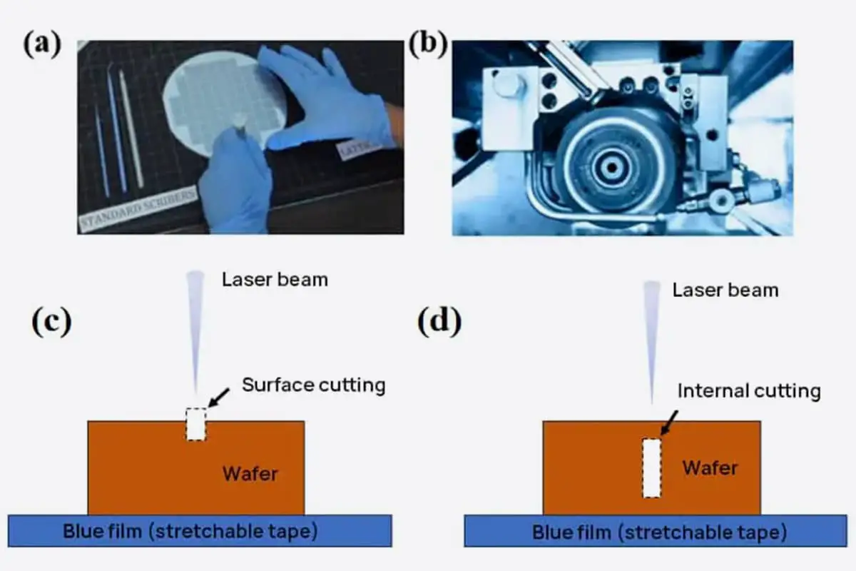
During the semiconductor chip manufacturing process, it is necessary to employ slicing techniques to dice wafers. However, traditional diamond cutting and grinding wheel cutting can cause significant damage to semiconductor materials, leading to issues such as wafer fragmentation and degradation of chip performance.
Consequently, the development of advanced cutting technologies holds immense significance for cost reduction and efficiency enhancement in the integrated circuit semiconductor industry. With the progress of laser technology, high-powered laser ablation cutting (i.e., laser slicing) and stealth dicing achieved using focused low-power lasers are gradually becoming mainstream chip dicing technologies.
Laser cutting is a non-contact processing method, which, unlike traditional diamond cutting and grinding wheel cutting, avoids chip-out, tool wear, water pollution, thermal effects, and chip trapping, which are significant issues.
However, the high-powered lasers used in laser ablation cutting generate substantial thermal effects during operation, which can easily damage the blue film at the bottom while cutting the wafer, thereby impacting the chip processing technique. Therefore, stealth dicing technology has gradually become a focal point in the semiconductor manufacturing industry.
Advanced Cutting: Detailed Explanation of Stealth Dicing Technology and Illustrative Applications
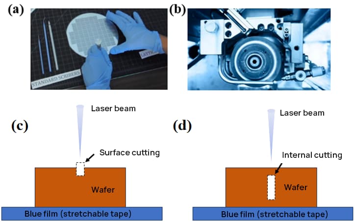
Stealth Dicing technology, by focusing a laser to form a small area of light spot, can generate enormous energy density, thereby achieving wafer cutting.
As a dry process, Stealth Dicing offers advantages such as high speed, high quality (no or very few chips), and low kerf loss. The specific process of Stealth Dicing can be divided into two steps:
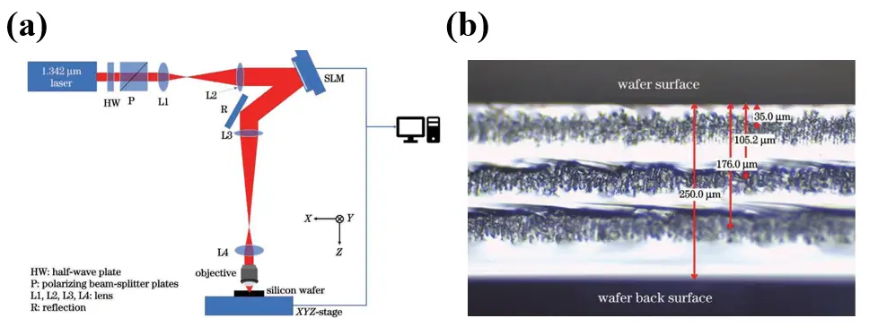
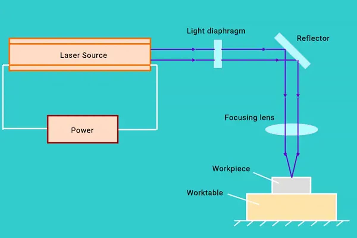
(1) Laser-induced perforation: As shown in Figure 2, a pulsed laser beam that can pass through the wafer is focused below the wafer surface by the optical system. When the laser power density at this focus point reaches its peak, a perforation is formed, and at this point, the chips on the wafer are not yet separated.
(2) Chip Separation: After unfolding the blue film placed on the wafer, due to the large tensile and compressive stresses present near the laser perforation, cracks can be induced along the laser path within the wafer, achieving chip separation.
Figure 2: Formation of perforation in the stealth cutting layer after laser focusing
Stealth laser cutting technology has now been applied in a variety of wafer cutting scenarios, such as:
(1) Silicon wafer cutting: When using conventional diamond blades to cut silicon, the thickness, granularity, rotation, and cutting speed of the blade significantly affect the quality of the cut. Despite years of technical improvements, the wide cutting width (kerf) caused by the blade still leads to material waste.
Additionally, the generation of debris and blade wear increase cutting costs. However, using stealth laser cutting technology with an ultra-narrow cutting path can eliminate the cost issues associated with additional debris cleanup and material waste, thereby improving chip productivity. Furthermore, by avoiding thermal damage, stealth laser cutting technology can further enhance the yield of chip manufacturing.
(2) Silicon carbide cutting: Silicon carbide is an ultra-hard material, second only to diamond in hardness, making it extremely difficult to machine. In the preparation of large size (6 inches and above) silicon carbide crystal substrate materials, stealth laser cutting technology, compared to fixed abrasive (diamond electroplated on steel wire) wire cutting technology, can improve the cutting efficiency by 3 to 5 times.
Given the significant issue of material consumption, stealth laser cutting technology can also increase the output rate of silicon carbide wafers by more than 30%.
(3) Special wafer cutting: When using stealth laser cutting technology to cut special wafers (for example, wafers with chip-mounting thin films or made of low-k materials), it is possible to avoid the generation of fractures and cracks, achieving high-efficiency, high-precision wafer cutting.
Figure 3: Display of Samples from Laser Stealth Cutting
Advancing Laser Stealth Cutting Technology
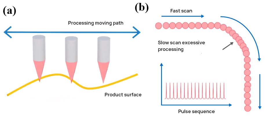
Despite the many advantages of laser stealth cutting technology, a series of issues still interfere with the cutting process. As shown in Figure 4, wafer surface warping and issues in managing laser energy density can prevent the laser focus from precisely landing on specific thin layers within the wafer, hindering improvements in cutting accuracy and chip yield rate.
Due to the difficulty in evenly applying the laser beam during acceleration, deceleration, and cornering stages, over-processing issues can easily occur. Additionally, problems such as analog interference, analog non-linearity, analog drift, or delays in the driver current loop will affect the control precision and responsiveness of the laser cutting platform.
In response to these issues, the academic and industrial sectors have proposed a series of solutions, as shown in Figure 5, which specifically include:
(1) Real-time height following control: During the wafer cutting process, displacement sensors are used to measure minute height fluctuations on the product surface in real time, and these are compensated in real time to the Z-axis where the laser is located, ensuring that the laser focus precisely lands on a specific thin layer in the wafer.
(2) High-speed position comparison output control: Development of a height following algorithm effectively avoids issues of excessive machining during laser acceleration, deceleration, and cornering, ensuring that the laser acts uniformly on the workpiece.
(3) PWM (Pulse Width Modulation) control technology: By directly outputting digital switch signals from the controller, which are then amplified through a power amplification module to directly control the motor current loop, a faster and more direct enhancement of the laser cutting platform’s control precision and responsiveness is achieved.
Figure 5: (a) The height following scheme used during wafer stealth dicing with laser; (b) Height data is collected at constant spatial intervals at all stages of the motion trajectory; (c) Motor current loop is controlled with digital signal.
Regarding the small action area and power tuning problem of single-focus laser stealth dicing, multi-focus laser stealth dicing technology has been specifically developed. This technique can simultaneously focus and generate multiple focal points inside the wafer for cutting, thereby significantly increasing cutting efficiency, as shown in Figure 6.
Figure 6: (a) Schematic of a multifocal stealth dicing apparatus, (b) Cross-section of a wafer post-multifocal laser stealth dicing.
During the process of multifocal laser stealth dicing, the position and intensity of the laser beam greatly influence the cutting quality. Due to the significant difference in refractive indices between air and semiconductor materials, the laser beam acting inside the wafer can cause a focal spot dispersion phenomenon, thus necessitating aberration correction.
To meet the wafer cutting needs in various application scenarios, people have been addressing these issues through technical breakthroughs, such as regulating the position and intensity of multiple foci and developing aberration correction technologies to overcome focal spot dispersion.
Laser Stealth Dicing Technology: A World of Greater Potential
Compared to traditional cutting technologies, laser stealth dicing holds notable advantages in practical applications, including significantly higher efficiency, superior quality, and lower loss.
By further optimizing and exploring laser stealth dicing technology, for example, through adjusting the beam energy during the stealth dicing process to achieve surface roughening of the photonic chip, or enhancing the efficiency of laser stealth dicing, we firmly believe that this technology will shine brightly in the field of integrated circuit semiconductor manufacturing, as well as other emerging domains.
As the founder of MachineMFG, I have dedicated over a decade of my career to the metalworking industry. My extensive experience has allowed me to become an expert in the fields of sheet metal fabrication, machining, mechanical engineering, and machine tools for metals. I am constantly thinking, reading, and writing about these subjects, constantly striving to stay at the forefront of my field. Let my knowledge and expertise be an asset to your business.
Lasers have revolutionized manufacturing, but do you know the top companies driving innovation in this field? In this blog post, we'll explore the key players shaping the future of laser…
Have you ever struggled with choosing the right laser cutting nozzle for your project? Selecting the optimal nozzle is crucial for achieving clean, precise cuts and maximizing efficiency. In this…
Have you ever wondered what makes a laser cutting machine tick? In this blog post, we'll dive deep into the inner workings of these high-precision machines that have revolutionized the…
Have you ever wondered how a laser can cut through metal like a hot knife through butter? In this fascinating article, we'll explore the science behind fiber laser cutting technology.…
Are you curious about the cutting-edge technology revolutionizing manufacturing? In this blog post, we'll dive into the world of laser cutting machines, exploring their advantages and the top manufacturers dominating…
Imagine the catastrophic consequences of neglecting laser cutting machine maintenance. Don't let your business fall victim to costly downtime and repairs! In this blog post, we'll dive into the essential…
Laser cutting revolutionized manufacturing, but even the most advanced machines encounter issues. In this blog post, we dive into common problems faced by laser plate cutting machines and provide step-by-step…
Intrigued by the art of laser cutting? This blog post dives deep into the critical parameters that make or break cut quality and efficiency. Discover insider tips from seasoned mechanical…
Curious about the capabilities of laser cutting? In this comprehensive guide, we'll dive into the world of laser cutting speeds and thicknesses for various metals. Our expert mechanical engineer will…