Have you ever wondered about the fascinating world of lithography machines? These marvels of engineering play a crucial role in the production of semiconductors, enabling the creation of intricate patterns on silicon wafers. In this article, we’ll explore the top lithography machine manufacturers, delving into their groundbreaking technologies and contributions to the industry. Get ready to discover the unsung heroes behind the devices we use every day.
Lithography machines play a crucial role in the semiconductor industry, as they enable the mass production of intricate microchips that power countless electronic devices.
As an individual keen on this subject, I understand that identifying the top manufacturers in this realm is essential for those looking to invest in or learn about the cutting-edge technology driving our world forward.
Consequently, I thought it would be useful to shed light on these leading lithography machine manufacturers and their contributions to the industry.
The global market for semiconductor lithography equipment continues to evolve, driven by the increasing demand for miniaturized and enhanced-performance electronic components.
In this context, I’ve observed that certain companies have emerged as frontrunners in the race to meet this need.
These manufacturers possess the expertise and innovation necessary to create advanced lithography machines capable of producing increasingly sophisticated chips, while also maintaining efficiency and cost-effectiveness.
In my research, I found several leading lithography machine manufacturers. These companies have made a significant impact in the field and continue to drive innovation in the semiconductor industry.
Here are the top lithography machine manufacturers I came across.

Country: Netherland
Founded: 1984
About the company:
ASML is a leading provider of technology solutions for the semiconductor industry, delivering the tools and services necessary for chip manufacturers to mass produce intricate patterns on silicon. Its customers are among the world’s top chip makers, who use ASML’s comprehensive product offering to produce a variety of semiconductor chips.
ASML offers a full range of hardware, software, and services to its clients, empowering them to increase their value and reduce costs in the chip-making process. With the ability to mass produce precise patterns on silicon, ASML’s customers are well-equipped to stay at the forefront of the industry.

Country: Japan
About the company:
Shanghai Nikon Precision Machinery Co., Ltd. specializes in providing after-sales service and consulting for semiconductor devices and flat panel display (FPD) optical equipment.
Integrated circuit chips and high-resolution FPDs are critical components in the advancement of the Internet of Things (IoT) and Artificial Intelligence (AI). Nikon is dedicated to research and development (R&D) and production of circuit diagram noise manufacturing systems for these components, contributing to the creation of an intelligent society.
The FPD noise device uses a circuit diagram to control each pixel by projecting it onto the surface of a glass substrate. Nikon offers a range of systems that are widely used in the industry, from large panels with unique multi-lens systems to small and medium-sized panels with intelligent devices.
With ongoing technical innovation, Nikon holds a significant market share in the FPD exposure system space. Semiconductor lithography equipment is used to shrink circuit graphics and project them onto chips, playing a crucial role in the production of integrated circuit chips. This exposure system requires high precision, with measurements as precise as nanometers, and is widely recognized as a highly sophisticated device.

Country: Japan
About the company:
Canon Optical Equipment (Shanghai) Co., Ltd. is a subsidiary of Canon established in mainland China to provide technical support and auxiliary services for the production of semiconductors and LCDs.
In addition to the semiconductor and LCD panel production light devices manufactured by Canon, the company also operates all semiconductor and LCD panel production equipment produced by Canon Machinery Company, Canon Anneihua Company, and Canon Special Machinery Company.
Canon’s involvement in the semiconductor and LCD panel production equipment business in mainland China dates back to the 1980s, when it started exporting low-end semiconductor exposure devices, such as proximity exposure devices and mirror projection exposure devices, to China. In the 1990s, it also supplied line steppers for semiconductor customers in Shanghai. The company’s offerings also include plasma degumming equipment and atmospheric pressure film forming equipment.
With the rapid growth of China’s semiconductor industry in the 21st century, Canon introduced high-end semiconductor exposure devices, such as KrF scanners, to the market. This was facilitated by a partnership with Mitsui Products Group, which broadened the reach of Canon’s products in China.
The company has also successfully expanded its presence in the market for LCD panel production equipment in China. Canon’s LCD panel exposure devices have consistently held a high market share since the inception of the Chinese LCD industry.
Canon is now prioritizing investment in Asia, particularly in the Chinese market, in advanced manufacturing fields such as semiconductors, LCD panels, and organic EL plates. In the future, as a part of the Canon group, the company will further enhance its support for customer enterprises by working closely with manufacturers and strive to improve customer satisfaction and grow its business.

Country: China
Founded: 2002
About the company:
Shanghai Smee Equipment (Group) Co., Ltd., also known as SMEE, is focused on the development, design, production, sales, and technical services of semiconductor equipment, pan-semiconductor equipment, and high-end intelligent equipment.
SMEE’s equipment is utilized in a range of manufacturing industries, including integrated circuit front-end, advanced packaging, flat panel display (FPD) panel, microelectromechanical systems (MEMS), light-emitting diodes (LEDs), power devices, and more.
The company is dedicated to providing its customers with high-quality products and technical services around the clock, striving to offer the best service and create outstanding value. SMEE is certified under the ISO27001 information security, ISO9001 quality management, and ISO14001 environmental management systems, and is committed to providing continuous, stable, and high-quality products and services, as well as fulfilling its responsibilities as a responsible high-tech enterprise.
Lithography is a critical technique in semiconductor manufacturing, enabling the creation of intricate patterns on silicon wafers. The process begins with applying a light-sensitive chemical known as photoresist onto the wafer. This photoresist reacts to light exposure, allowing selective areas to be hardened or softened, which can then be developed to form a pattern.
Light sources used in lithography include ultraviolet (UV) light, deep ultraviolet (DUV) light, and extreme ultraviolet (EUV) light. EUV lithography utilizes light with a wavelength of 13.5 nanometers, much shorter than traditional UV light, enabling the creation of finer patterns crucial for advanced microchips.
Lithography machines incorporate sophisticated mechanical and optical systems to achieve precision and efficiency.
Modern lithography machines often use the step-and-scan method. In this method, the wafer and reticle stages move continuously in sync during exposure, enhancing productivity and yield rates. High-throughput lithography systems can process hundreds of wafers per hour, each containing thousands of individual chips. This capability is essential to meet global demand for electronic devices and support the rapid growth of technology markets.
Lithography equipment is fundamental in the production of semiconductor devices. Advanced techniques such as Extreme Ultraviolet (EUV) and Deep Ultraviolet (DUV) lithography enable the creation of microchips with billions of transistors. For example, companies like Intel and TSMC use EUV lithography to produce their latest 7nm and 5nm chips, which power high-performance computing devices like the Apple M1 processor. As the demand for smaller, more powerful chips increases, lithography continues to drive innovation in this sector.
The automotive sector increasingly relies on sophisticated semiconductor devices to enhance vehicle performance and safety. Lithography machines are crucial for manufacturing high-performance sensors and chips used in electric vehicles (EVs) and advanced driver assistance systems (ADAS). Features such as automatic braking and lane-keeping assistance are made possible by these technologies. For instance, Tesla’s Full Self-Driving (FSD) system relies heavily on chips produced using advanced lithography.
In telecommunications, the rollout of 5G technology has created a significant demand for advanced semiconductor devices capable of handling increased data speeds and connectivity. Lithography equipment is critical in producing the complex chips required for 5G infrastructure, including base stations and mobile devices. This technology supports the global expansion of 5G networks, facilitating faster internet access and improved communication services.
In consumer electronics, lithography is used to produce components for devices like high-definition displays, smart home devices, and other consumer gadgets. The precision offered by lithography enables the creation of high-resolution screens and efficient processors. For example, the OLED displays in the latest smartphones are manufactured using lithographic techniques, allowing for vibrant colors and deep blacks.
Lithography plays an essential role in advanced packaging technologies, such as 2.5D and 3D IC packaging, which allow for the integration of multiple chips into a single package. Additionally, it is vital in the production of Micro-Electro-Mechanical Systems (MEMS), which encompass a range of applications from sensors to actuators. MEMS devices are increasingly used in industries such as healthcare, automotive, and consumer electronics, where miniaturization and precision are critical. For instance, MEMS accelerometers and gyroscopes are key components in smartphones and wearable devices.
As artificial intelligence (AI) and the Internet of Things (IoT) gain traction, lithography machines are crucial in fabricating the high-performance chips needed for these technologies. These devices must be compact and efficient, enabling real-time data processing and connectivity in smart devices, home automation systems, and industrial applications. Companies like NVIDIA utilize advanced lithography to produce GPUs that power AI applications, enhancing machine learning algorithms and IoT functionalities.
The transition to Industry 4.0, characterized by automation and smart manufacturing, relies on advanced semiconductor components produced through lithography. These components are integral to the development of robotics, wireless control systems, and smart machinery, ensuring high precision and reliability in modern production environments. For example, industrial robots used in assembly lines are equipped with sensors and processors fabricated using lithographic techniques, enabling precise and efficient operation.
Lithography machines are indispensable across multiple industries, facilitating the creation of advanced technologies that drive innovation and efficiency in our increasingly interconnected world.
Below are answers to some frequently asked questions:
The top lithography machine manufacturers in the semiconductor production sector are led by a few key players due to the high technological barriers and significant investment required in this field. ASML Holding NV stands out as the most dominant player, particularly in the extreme ultraviolet (EUV) lithography market. Established in 1984, ASML specializes in photolithography machines and has shipped around 140 EUV systems as of 2022, holding a near-monopoly in this segment. The company is also developing next-generation EUV systems expected to support high-volume chip manufacturing starting in 2025-2026.
Canon Inc. is another major player with over 50 years of experience in semiconductor lithography. Recently, Canon launched the “Lithography Plus1” solution platform and introduced an i-line lithography stepper designed for advanced packaging processes.
Nikon Corporation remains a significant competitor, offering a range of lithography systems, although it does not match ASML’s dominance in EUV technology. Veeco Instruments Inc. also plays a role in the semiconductor lithography equipment market, providing various types of lithography and process equipment, but with less emphasis on EUV.
SÜSS MicroTec SE, based in Germany, specializes in semiconductor manufacturing equipment, including lithography systems, and maintains a notable presence in the broader lithography market.
Other notable players include Carl Zeiss AG, known for its optical components and contributions to EUV lithography, TOPPAN Inc., which focuses on photomask solutions, and NTT Advanced Technology Corporation, which is emerging in the EUV technology space. Collectively, these companies drive advancements in the semiconductor lithography market, with ASML Holding NV clearly leading the EUV segment.
ASML’s Extreme Ultraviolet (EUV) lithography systems are at the forefront of semiconductor manufacturing, providing advanced technical capabilities essential for producing the most sophisticated microchips. These systems use light with a wavelength of 13.5 nanometers, significantly shorter than the Deep Ultraviolet (DUV) light, allowing for the creation of extremely small and precise features on silicon wafers. This enables the production of smaller, faster, and more powerful chips.
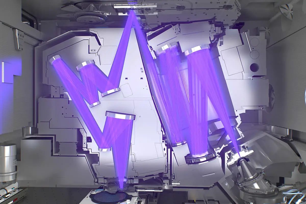
The EUV light is generated using a laser-produced plasma (LPP) source, where molten tin droplets are vaporized by powerful laser pulses to create a plasma that emits EUV light. This process is repeated 50,000 times per second. The EUV lithography involves directing the light through a series of precision mirrors to focus and shape the beam before it illuminates a photomask with the desired circuit patterns. Advanced mechatronics engineering ensures the precise synchronization of the mask and wafer movements, achieving high-speed and high-precision pattern transfer without causing vibrations.
The production of EUV machines involves a complex supply chain with over 5,100 unique suppliers, requiring intelligent integration of computational lithography, lithography systems, and metrology and inspection. These machines are crucial for manufacturing the latest generation of microchips used in AI, smartphones, supercomputers, self-driving vehicles, and medical devices.
EUV machines are large and costly, with each unit averaging around €150 million in 2023, and the next-generation High NA EUV machine expected to cost about $350 million. They demand substantial resources, including high electrical power consumption, large cooling water flow rates, and specific gas line requirements. Despite challenges related to tool uptime and throughput, the wafer exposure throughput has improved, reaching up to 1,000 wafers per day per system.
Overall, ASML’s EUV systems are characterized by their advanced technical specifications, high performance in producing intricate microchip patterns, and ongoing improvements in productivity, making them indispensable in the semiconductor industry.
The lithography machine market is characterized by intense competition and high concentration, with a few key players dominating the industry. ASML Holding N.V. stands out as the market leader, particularly due to its exclusive capability to produce extreme ultraviolet (EUV) lithography equipment, essential for cutting-edge semiconductor manufacturing. Other significant competitors include Nikon Corporation, known for its advanced deep ultraviolet (DUV) lithography equipment, and Canon Inc., which has a longstanding presence in the semiconductor lithography space and continues to innovate with technologies like “Lithography Plus1.”
Veeco Instruments Inc. also contributes to the market with specialized lithography solutions, alongside other notable companies such as SÜSS MicroTec SE, Ultratech Inc., Toppan Printing Co. Ltd., SCREEN Holdings Co. Ltd., and Vistec Semiconductor Systems GmbH. These companies employ various competitive strategies to maintain and grow their market share, including mergers and acquisitions, joint ventures, new product launches, and strategic alliances.
Regional dynamics play a significant role in market competition, with Asia Pacific expected to experience the highest growth rate due to major semiconductor foundries like TSMC, Samsung, and SMIC. Europe remains a critical hub for advanced lithographic technology, largely due to ASML’s presence, while North America also holds a significant position driven by its robust semiconductor sector.
Despite the competitive landscape, challenges such as the high cost of EUV lithography systems, which can reach approximately $120 million, pose potential constraints on market growth. These systems’ complexity and high price make them a significant investment, impacting the overall market dynamics.
Lithography machines are predominantly used in several key industries due to their essential role in semiconductor manufacturing. The primary industry is the semiconductor industry, where these machines are vital for fabricating integrated circuits by transferring circuit patterns onto silicon wafers. This process is crucial for producing chips with billions of transistors, which are foundational components in a wide array of electronic devices.
In the consumer electronics industry, lithography machines are critical for producing advanced chips used in smartphones, laptops, and smart home devices. The miniaturization and enhanced functionality achieved through advanced lithography techniques are crucial for the performance and efficiency of these devices.
The automotive industry also heavily relies on lithography machines for manufacturing advanced semiconductors used in autonomous vehicles, safety systems, and infotainment systems. These machines are used to produce chips with both advanced and larger features suitable for various automotive applications.
In telecommunications, particularly with the rollout of 5G technology, lithography machines are indispensable for creating the high-performance semiconductors required for 5G infrastructure and devices.
Furthermore, the Internet of Things (IoT) and Industry 4.0 technologies depend on lithography machines for producing the sophisticated semiconductors that power smart devices, machines, and robots. These industries benefit from the capabilities of lithography to produce highly integrated and efficient semiconductor components.
Overall, lithography machines are critical across multiple industries, driving innovation and supporting the development and functionality of a wide range of advanced technologies.
ASML Holding N.V., known simply as ASML, is a prominent player in the semiconductor industry, recognized for its advanced photolithography machines. The company was established on April 1, 1984, as a joint venture between Royal Philips Electronics and ASM International, under the name ASM Lithography. This collaboration aimed to commercialize a wafer stepper developed at Philips and was supported by the Dutch Ministry of Economic Affairs.
By 1988, ASML had become independent from ASM International, and in 1993, it also severed ties with Royal Philips Electronics, allowing it to concentrate solely on developing and manufacturing lithography systems. A significant breakthrough came in 1991 with the release of the PAS 5500 lithography system, which established ASML as a competitor to industry giants like Canon and Nikon.
ASML began exploring extreme ultraviolet (EUV) lithography in the late 1990s, working with partners such as Intel and the US Department of Energy. This research required substantial investment, totaling over $6.3 billion over 17 years. Key acquisitions and partnerships have been crucial to ASML’s growth: in 2000, it acquired the Silicon Valley Group, and in 2012, Intel invested $4.1 billion to expedite EUV development. That same year, ASML acquired Cymer, a manufacturer of DUV and EUV sources, and in 2016, it purchased Hermes Microvision Inc. to enhance its technology for smaller semiconductors.
ASML is listed on both the Euronext Amsterdam and NASDAQ stock exchanges and has become one of Europe’s most valuable companies, with a market capitalization of about $264 billion as of November 2024. It operates globally, employing over 42,000 people from 143 nationalities and relying on nearly 5,000 tier 1 suppliers.
Despite challenges such as a significant drop in sales during the 2008 financial crisis and intellectual property theft in 2015, ASML has consistently rebounded by maintaining strategic R&D investments. Today, ASML is the largest supplier to the semiconductor industry and the sole provider of EUV photolithography machines, essential for producing the most advanced chips. The company’s success is driven by its innovation, strategic partnerships, and substantial R&D investments, securing its leading position in the lithography market.

