How does modern manufacturing achieve nearly perfect precision? Ultra-precision machining techniques enable astonishing accuracy, reaching sub-micron and nanometer levels. This article explores methods like ultra-precision cutting, grinding, lapping, and special processing technologies. Readers will learn about the tools and technologies that make such precision possible, and the industries benefiting from these advancements.
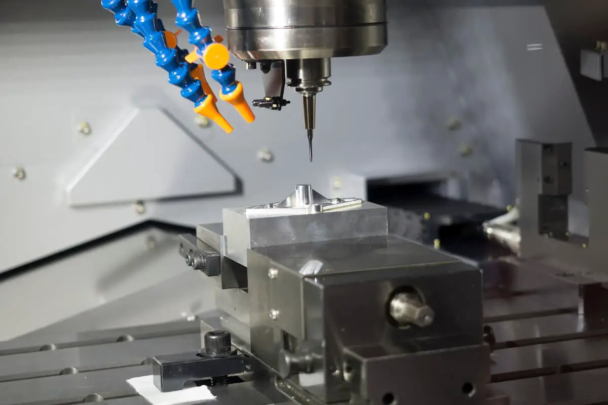
Ultra-precision machining refers to precision manufacturing processes that achieve extremely high levels of accuracy and surface quality. Its definition is relative, changing with technological advancements.
Currently, this technique can achieve sub-micron and even nanometer-level dimensions and shapes, with a surface roughness at the nanometer scale. Ultra-precision machining methods include ultra-precision cutting (such as ultra-precision turning and milling), ultra-precision grinding, ultra-precision lapping, and ultra-precision special processing.
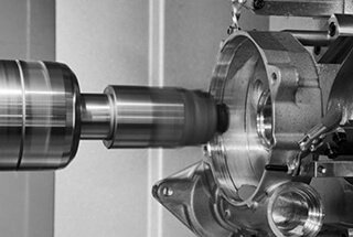
Ultra-precision cutting primarily involves turning with diamond tools, mainly used for machining non-ferrous alloys, optical glass, marble, and non-metallic materials like carbon fiber boards. The high precision achieved in ultra-precision cutting is due to the low affinity between diamond tools and non-ferrous alloys, along with their excellent hardness, wear resistance, and thermal conductivity.
Furthermore, in ultra-precision cutting, high-precision air bearings, air-floating guides, positioning detection components, and measures like constant temperature, vibration isolation, and vibration damping are adopted.
This ensures a surface roughness Ra value of less than 0.025μm and a geometric precision up to 0.1μm, making ultra-precision cutting increasingly popular in aerospace, optics, and civilian applications, moving towards higher precision.
Ultra-precision grinding is a sub-micron level processing method, progressing towards the nanometer level. It refers to a grinding method that achieves a processing precision of 0.1μm or higher and a surface roughness Ra value below 0.025μm, suitable for processing hard and brittle materials like steel, ceramics, and glass.
Traditional grinding and polishing processes can be eliminated through ultra-precision grinding to achieve the required surface roughness. Besides ensuring accurate geometric shapes and dimensions, mirror-like surface roughness can be obtained through ultra-precision grinding.
Ultra-precision lapping includes mechanical lapping, chemo-mechanical lapping, float lapping, elastic emission machining, and magnetic lapping. The spherical runout tolerance of parts processed by ultra-precision lapping can reach 0.025μm, and the surface roughness Ra value can reach 0.003μm.
Key conditions for ultra-precision lapping are precise temperature control, vibration-free processing, a clean environment, and small, uniform abrasive particles. High-precision detection methods are also indispensable.
Ultra-precision special processing technology is internationally recognized as one of the most promising technologies of the 21st century. It refers to processing methods that use energy forms like electrical, thermal, optical, electrochemical, chemical, acoustic, and special mechanical energy to remove or add material.
The primary objects of application include difficult-to-process materials (like titanium alloys, heat-resistant stainless steel, high-strength steel, composites, engineering ceramics, diamond, ruby, hardened glass, and other high-hardness, high-toughness, high-strength, high-melting point materials), difficult-to-process parts (like complex three-dimensional cavities, holes, group holes, and narrow slots), low-rigidity parts (like thin-walled parts, elastic elements), and processes that achieve welding, cutting, hole making, spraying, surface modification, etching, and fine processing with high energy density beams.
These processing methods include laser processing technology, electron beam processing technology, ion beam and plasma processing technology, electrical processing technology, etc., with only a brief introduction here.
Laser processing involves a laser generator focusing high-energy-density laser light onto the surface of a workpiece. The absorbed light energy instantaneously transforms into thermal energy, which, based on its density, can achieve hole punching, precision cutting, and the production of micro anti-counterfeit marks.
With the rapid development of laser processing equipment and technology, over 100kW high-power lasers and kilowatt-level high-beam solid-state lasers have emerged, equipped with optical fiber for multi-station, long-distance work.
Due to the high power and automation level of laser processing equipment, CNC control and multi-coordinate linkage are widely adopted, equipped with auxiliary systems like laser power monitoring, automatic focusing, and industrial television display. Currently, the minimum hole diameter achieved by laser drilling is 0.002mm, the speed of laser cutting thin materials can reach 15m/min, and the cutting gap is only between 0.1-1mm.
Applications of laser surface strengthening, surface remelting, alloying, amorphous processing technology are becoming increasingly widespread, and laser micro-processing in electronics, biology, and medical engineering has become an irreplaceable special processing technology.
Electron beam processing involves continuously emitting negative electrons from the cathode to the anode in a vacuum. The electrons accelerate and focus into a very thin, high-energy-density electron beam during the transition from the cathode to the anode. When high-speed electrons hit the surface of the workpiece, their kinetic energy turns into thermal energy, causing the material to melt and vaporize, then be removed from the vacuum.
Controlling the strength and deflection direction of the electron beam, combined with the numerical control displacement of the workbench in the x and y directions (using CNC control and multi-coordinate linkage), can achieve punching, forming cutting, etching, photolithography exposure, and other processes.
Electron beam processing technology is maturing internationally and is widely used for the combination welding of large structures of main load-bearing components like launch rockets and spacecraft, as well as the manufacturing of important structural parts like aircraft beams, frames, landing gear components, engine integral rotors, casings, power shafts, and nuclear power device pressure vessels.
Integrated circuit manufacturing also widely adopts electron beam photolithography exposure, which has a much shorter wavelength than visible light, achieving a line pattern resolution of 0.25μm.
Ion beam processing involves accelerating and focusing ions produced by an ion source in a vacuum to hit the surface of a workpiece. Compared to electron beam processing, since ions carry a positive charge and their mass is millions of times larger than electrons, they can gain greater kinetic energy after acceleration.
They rely on microscopic mechanical impact energy rather than converting kinetic energy into thermal energy to process the workpiece. Ion beam processing can be used for surface etching, ultra-clean cleaning, and atomic/molecular level cutting.
Micro electrical discharge machining involves the removal of metal in an insulating working fluid through a localized high temperature caused by a pulse spark discharge between a tool electrode and a workpiece. The process doesn’t involve macroscopic cutting forces; precise control of single pulse discharge energy combined with precise micro-feed can remove extremely fine metal materials.
It can process microshafts, holes, narrow slots, flat and curved surfaces. High-end EDM shaping and wire cutting can provide micrometer level processing precision, capable of processing a 3um microshaft and a 5μm hole.
Micro electrolytic processing involves decomposing water into hydrogen ions and hydroxyl ions in a conductive working fluid. The metal atoms on the surface of the workpiece, serving as an anode, become metal cations and dissolve into the electrolyte, being gradually electrolyzed. These then react with the hydroxyl ions in the electrolyte to form metal hydroxide precipitates, while the tool cathode does not wear.
There are also no macroscopic cutting forces between the tool and the workpiece in the processing process. By precisely controlling the current density and electrolysis location, nanometer-level precision electrolytic processing can be achieved, and the surface will not have processing stress.
Micro electrolytic processing is often used for mirror polishing, precision thinning, and situations requiring stress-free processing. Electrolytic processing applications are broad, extending from blades and integral impellers to casings, disk ring components, and deep small hole processing.
High-precision metal reflective mirrors can be processed using electrolytic processing. Currently, the maximum current capacity of electrolytic processing machines has reached 50,000A, and CNC control and multi-parameter adaptive control have been implemented.
Composite processing refers to processing technologies that use several different forms of energy and methods, combining their advantages, for example, electrolytic grinding, ultrasonic electrolytic processing, ultrasonic electrolytic grinding, ultrasonic electrical discharge, ultrasonic cutting, etc.
Composite processing is more effective and has a broader application range than single processing methods.
