Have you ever wondered how the quality of welding impacts the reliability of electronic products? In welding, even a minor flaw can lead to significant failures. This article explores the key standards and inspection methods to ensure welding quality, covering aspects like electrical and mechanical integrity, appearance, and inspection techniques. By the end, you’ll understand how to identify and prevent common welding defects, ensuring robust and reliable electronic assemblies. Dive in to discover how mastering these standards can safeguard your products from costly malfunctions.
Welding is a significant technological process in the assembly of electronic products and is a pivotal stage in their manufacture.
It is extensively used in the experimentation, adjustment, and production of electronic products and constitutes a substantial workload. The quality of welding directly influences the quality of the product.
Most failures in electronic products, besides component issues, are predominantly due to poor welding quality. Therefore, mastering proficient welding operation skills is essential for product quality.
I. Quality Requirements for Welding Points
The quality requirements for welding points should encompass good electrical contact, sturdy mechanical contact, and aesthetic appearance.
The most critical aspect of ensuring welding point quality is to avoid cold solder joints.
1. Reliable electrical connection
Welding is the primary means of physically realizing electrical connections in electronic circuits. Soldering connections are not achieved by pressure, but by forming a solid alloy layer during the welding process to achieve the purpose of electrical connection.
If the solder is merely stacked on the surface of the welded parts or only a small part forms an alloy layer, it may be difficult to detect any problems with the welding point during the initial tests and operation.
Such a welding point may pass current in the short term, but with changes in conditions and the passage of time, the contact layer oxidizes, separates, and creates intermittent or non-working circuits.
Observing the exterior of the welding point may still seem fine, which is a major concern during the use of electronic instruments and a problem that must be taken seriously during product manufacturing.
2. Adequate mechanical strength
Welding not only serves the purpose of electrical connection but also fixes components and ensures mechanical connection. To ensure that the welded parts do not fall off or loosen when subjected to vibration or impact, the welding points must have adequate mechanical strength.
Generally, this can be achieved by bending the lead terminals of the components to be welded and then performing the welding.
Lead-tin alloy, used as soldering material, has relatively low strength, with the tensile strength of commonly used lead-tin soldering materials being about 3-4.7kg/cm2, only 10% of ordinary steel.
To increase strength, a sufficient connection area is required. If it’s a cold solder joint with the solder merely piled on the solder pad, it won’t have any strength.
3. Smooth and neat appearance
A good welding point requires an appropriate amount of solder, has a metallic luster, doesn’t have spikes or bridges, and doesn’t damage the insulation layer of the wire or adjacent components. A good appearance reflects the quality of the welding.
Note: The presence of a metallic shine indicates appropriate welding temperature and the formation of an alloy layer, which is not just a requirement for aesthetic appearance.
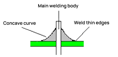
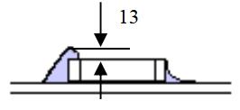
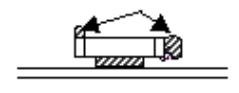
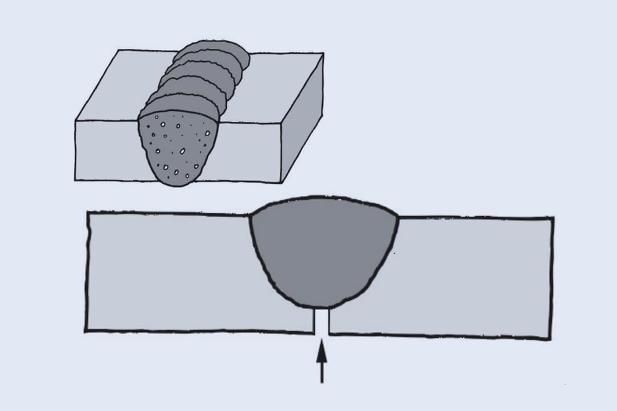
The appearance of a typical weld point is depicted in Figure 1, with the following common characteristics:
The shape is symmetrically skirt-like, centered around the welding wire.
The welding material forms a semi-arched concave surface, with a smooth junction between the weld material and the welded part, and the contact angle is as small as possible.
The surface is glossy and smooth.
There are no cracks, pinholes, or slag inclusions.
Figure 1
In addition to visual inspection (or using a magnifying glass or microscope) to check if the weld point meets the above standards, the inspection of the welding quality also includes the following: missing welds; spiky solder; solder-induced short circuits between wires (i.e., “bridging”); damage to wire and component insulation; wire shaping; solder splashing.
During inspection, in addition to visual checks, methods such as touch, tweezer probing, and wire pulling are used to check for defects such as wire breakage and pad peeling.
II. Welding Quality Inspection Methods
1. Visual inspection
Visual inspection involves checking the welding quality from an external perspective to identify any defects in the weld point.
The main content of visual inspection includes:
1. Whether there are missing welds, i.e., weld points that should be soldered are not.
2. The luster of the weld point.
3. Whether there is sufficient solder at the weld point.
4. Whether there are residual fluxes around the weld point.
5. Whether there are continuous welds and whether the pads have slipped off.
6. Whether the weld point has cracks.
7. Whether the weld point is uneven; whether there is a spiky phenomenon at the weld point.
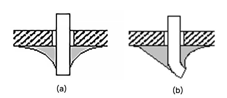
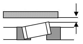
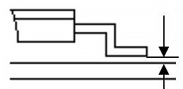
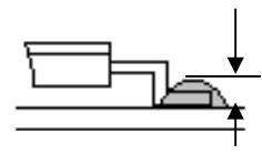
Figure 2: Correct Cross-Section of a Weld Point
Figure 2 shows the correct weld point shape. In the figure, (a) is the shape of a straight-inserted weld point, and (b) is the shape of a semi-bent weld point.
2. Touch inspection
Touch inspection mainly refers to whether there are loose or insecurely welded components when touched.
Using tweezers to hold the component lead and gently pulling on it to see if there is any looseness. Whether the solder on top falls off when the weld point is shaken.
3. Power-on inspection
After the external inspection is completed and the wiring is confirmed to be correct, power-on inspection can be conducted, which is key to testing circuit performance.
If the external inspection is not rigorously conducted, power-on inspection will not only be more difficult, but it may also damage equipment and cause safety accidents.
For instance, if the power supply connection is not soldered well, it would be discovered that the device cannot be powered on during power-on inspection, making checking impossible.
Power-On Inspection and Root Cause Analysis
Electrification Inspection
(1) Component failure
Failure: The soldering iron is experiencing electrical leakage and has suffered damage due to overheating.
Performance degradation: The soldering iron has an electrical leakage issue and has been damaged due to overheating.
(2) Poor electrical conductivity
Short circuit: Bridging and solder splatter.
Circuit Interruption: Solder joint opens, rosin flux residue, cold soldering, and poor contact in sockets.
Intermittently connected: Wire breakage, pad peeling, and so forth.
Power-on inspections can reveal many minor defects, such as circuit bridging that is not visible to the naked eye. However, it is challenging to detect potential issues like internal dry soldering.
Therefore, the fundamental solution lies in improving the skill level of the welding operation, rather than leaving the task to the inspection process.
The relationship between potential faults that may occur during power-on inspection and welding defects is illustrated in Figure 3 for reference.
III. Common PCBA Solder Joint Defects and Analysis
There are numerous causes of welding defects. Given certain materials (solder and flux) and tools (soldering iron, jig), the methods employed and the operator’s sense of responsibility become determining factors.
The common defects seen in PCBA component positioning and solder joints are shown in Tables 1 and 2.
These tables list the appearance, characteristics, and hazards of common solder joint defects, along with an analysis of their causes.
Table 1: Analysis of Common Solder Joint Defects
Welding point defect
Design Characteristics
Harm
Root Cause Analysis
False Welding
There is a distinct black line between the solder and the lead of the component or the copper foil, with the solder receding towards the boundary.
Cannot function properly.
1. The component leads were not properly cleaned, inadequately tinned, or the solder has oxidized.
2. The printed circuit board was not thoroughly cleaned, and the quality of the applied flux was subpar.
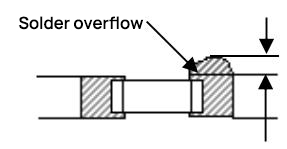
Solder short circuit
Excessive soldering has led to a short circuit due to solder bridging between adjacent points.
1. The component leads are left too long after cutting.
2. Residual component leads have not been cleared.
Scratch movement welding
There are cracks, rough as crumbled bread, with gaps at the joints.
The strength is low, it’s either not functioning or intermittently operational.
When the solder is still wet and subjected to movement.
Insufficient solder
The welding area is less than 75% of the pad, and the solder has not formed a smooth overplated surface.
Insufficient mechanical strength.
1. Poor solder flow or premature withdrawal of the welding wire.
2. Insufficient flux.
3. Welding duration is too short.
Excessive solder
The surface of the solder is convex.
Wasting solder could potentially conceal defects.
Wire withdrawal was delayed.
Overheating
The weld spot appears white, lacking metallic lustre, with a rather coarse surface.
The solder pad is prone to peeling, resulting in reduced strength.
The soldering iron’s power is excessive, resulting in prolonged heating times.
Cold soldering
The surface presents itself as tofu-like granules, and at times, there may be cracks.
The strength is low, and the conductivity is poor.
Stir the workpiece before the solder solidifies.
No wicking
When the contact angle exceeds 90 degrees, the solder cannot spread or cover, similar to a droplet of oil resting on a surface with moisture.
The strength is low, and the conductivity is poor.
The soldered metal surfaces are not symmetrical, and neither is the heat source itself.
Looseness
The leads of wires or components may shift.
Poor conductivity or no conductivity.
1. The lead moved before the solder had solidified, causing a gap.
2. The lead was not treated (poor wetting or no wetting).
Pulling to a point
Emergence of the cutting edge.
The appearance is subpar, which can easily lead to bridging occurrences.
An unclean soldering iron, or one removed prematurely before the soldering site reaches the solder’s melting point, can result in solder adherence and subsequent formation as it’s withdrawn.
Pinhole
Visual inspection or a low-power magnifier can reveal holes in the copper foil.
Insufficient strength can lead to weld points being prone to corrosion.
The contamination of soldering materials, part materials, and the environment.
Copper foil delamination
The copper foil is peeled off from the printed circuit board.
The circuit board has been damaged.
The welding duration is too long.
Table 2: Standard and Defect Analysis of SMT Solder Joints for Surface-Mounted Components.
Project
Diagram
Key Points
Inspection Tools
Judgment Criteria:
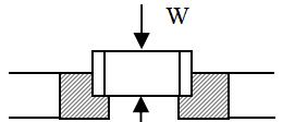
1. Position of the part.
The amplitude ‘W’ of the joint electrode covers over half of the conducting surface. Important: Visual inspection should be used to identify the offset of the component’s position, not through verification with a tester. Instead, use a magnifying glass for direct observation.
Calipers
More than half
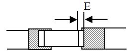
2. Position of the part.
More than half of the length E of the joint electrode is covered on the conducting surface. Precaution: Visual inspection should be used to determine the offset of the part’s position, not confirmed with a tester and checked by magnifying glass.
Calipers
More than half
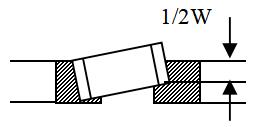
3. Position of the part.
In terms of the tilt of the joint parts, it suffices to cover more than half of the amplitude W of the joint electrode on the conductive surface. Note: Rely on visual inspection for part positioning discrepancies, and avoid using a tester for confirmation; instead, use a magnifying glass for direct observation.
Calipers
More than half
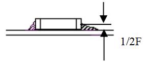
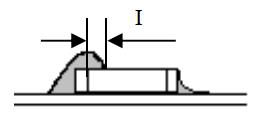
4. Amount of solder.
1/2F
The electrode is soldered with tin, the extent of which exceeds half the height F and half the width W.
Calipers
More than half
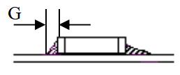
5. Amount of solder.
Solder the joint components in the longer direction, from the end face of the joint electrode, with a solder thickness of more than 0.5mm. For example, G.
Calipers
Above 0.5mm
6. Amount of solder.
The height of the solder should be less than 0.3mm above the surface of the joint component.
Dial Indicator
Below 0.3mm
7. Amount of solder.
The soldering on the joint parts cannot be overlapped, like in the form of “I”.
Visual Inspection
Cannot be stacked on top
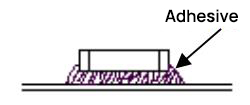
8. Adhesion of the part.
Quality Product
There is no adhesive between the electrode of the joint component and the printed circuit board.
Visual Inspection
Cannot be under the electrode
Quality Product
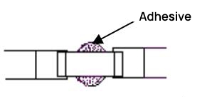
9. Adhesion of the part.
Defective product
There is no adhesive between the electrode of the joint component and the printed circuit board.
Visual Inspection
Cannot be under the electrode
10. Adhesion of the part.
Must not contain any binders.
Adhesives must not be applied to the electrode section of the joint components.
Visual Inspection
Cannot be adhesive
11. Position of the part.
Do Not Touch G
The positioning of the joint components should not be offset or tilted to touch adjacent conductors. For aspects that cannot be determined visually, use testing instruments.
Visual Inspection
Cannot make contact
12. Amount of solder.
Solder overflow
Solder must not overflow beyond the width of the conductive surface.
Visual Inspection
Cannot overflow
13. Position of the part.
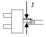
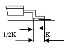
More than half of the width J of the IC component’s legs is above the conducting surface.
Calipers
More than half
14. Position of the part.
Over half of the length, K, of the IC component’s legs makes contact above the conducting surface.
Calipers
More than half
15. Position of the part.
The displacement of the component position relative to the adjacent conductor should be ≥0.2mm; it must not make contact with the adjacent conductor.
Visual Inspection
Cannot make contact
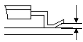
16. Unstable leg.
For items with uplifted tip ends, the uplift should be less than 0.5mm.
Calipers
Below 0.5mm
17. Unstable leg.
For items where the base is lifted, the lift at the base should be less than 0.5mm.
0.5mm Gauge
Below 0.5mm
18. Unstable leg.
For items where the entire foot is raised, the elevation should be less than 0.5mm.
0.5mm Gauge
Below 0.5mm
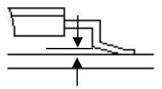
19. Unstable leg.
The height of the solder from the surface of the printed board to the peak of the solder is less than 1mm.
Calipers
Below 1mm
20. Unstable leg.
The height of the solder attached to the component leg is under 0.5mm.
As the founder of MachineMFG, I have dedicated over a decade of my career to the metalworking industry. My extensive experience has allowed me to become an expert in the fields of sheet metal fabrication, machining, mechanical engineering, and machine tools for metals. I am constantly thinking, reading, and writing about these subjects, constantly striving to stay at the forefront of my field. Let my knowledge and expertise be an asset to your business.
Have you ever wondered how modern factories maintain top-notch welding quality? In today’s world, welding robots are the answer. This article explores the advanced technologies behind these robots, like real-time…
Welding technology is a prevalent technique in the field of mechanical manufacturing and has been extensively applied in various stages of industrial production. It plays a pivotal role in promoting…
Welding defects can be catastrophic, leading to structural failures and safety hazards. But how can you ensure your welds are flawless? This article delves into essential welding quality inspections, covering…
Ever wondered how to improve welding quality for 6-series aluminum alloys? This article delves into optimizing MIG spot welding, comparing different welding parameters and techniques. Discover how changes in groove…
How do the various metal elements in welding wire impact the final weld quality? From silicon to vanadium, each element plays a unique role in the welding process. Understanding their…
How can you ensure the welding rods you're using are of high quality? This article introduces straightforward methods for checking welding rod quality, including visual inspection, testing coating strength, and…
What do the colors of titanium weld seams reveal about their quality? This fascinating question delves into the intricacies of welding titanium, a metal known for its reactivity and unique…
Achieving a flawless weld requires more than just skill; it hinges on mastering the interplay between voltage and current. These two parameters are the lifeblood of welding, dictating everything from…
Have you ever wondered why welded structures sometimes fail despite their robust appearance? This article dives into the hidden challenges of welding, exploring how uneven heating and cooling can lead…